IMX6-CycloneV interface description
Page under construction...
 Informations on this page are not guaranteed !!
Introduction
This article describe the bus interface configuration to communicate between i.MX6 processor and CycloneV FPGA. In i.MX6, the bus used to make communication with the FPGA is the PCI express.
PCIe
PCIe used to do the communication between i.MX6 and CycloneV is a Gen1 with one lane. By defaut, Armadeus recommend to use the quartus ip-core Cyclone V Avalon-MM Interface for PCIe.
Simplified view
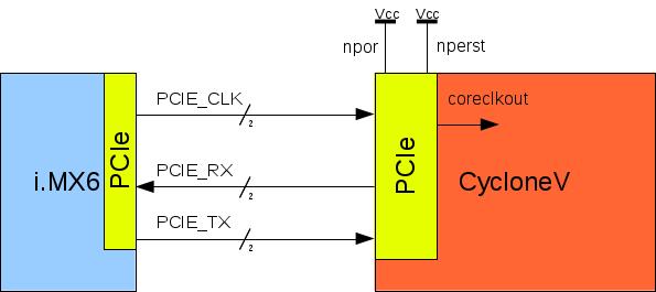
Figure 1 is a simplified view of APF6 schematics, signals are :
- PCIE_CLK: 125Mhz differential pcie clock (PCIE_CLKN and PCIE_CLKP).
- PCIE_RX: Differential receive pcie signal lane0 (PCIE_RXN and PCIE_RXP).
- PCIE_TX: Differential transmit pcie signal lane0(PCIE_TXN and PCIE_TXP).
- npor: set to Vcc.
- nperst: set to vcc.
- coreclkout: 125Mhz (by default) clock generated by quartus hard PCIe ip-core, used to clock design by defaut.
Qsys (Quartus) : Avalon-MM Cyclone V Hard IP for PCI Express configuration (CvP)
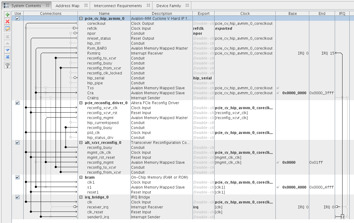
3 Qsys components are required to use PCIe on apf6sp with configuration via PCIe:
- Avalon-MM Cyclone V Hard IP for PCI Express : The hard ip for PCIe
- Altera PCIe Reconfig Driver
- Transceiver Reconfiguration Controller
Avalon-MM Cyclone V Hard IP for PCI Express
To use the Altera IP on the APF6_SP configure it as following :
- Number of lanes : x1
- Enable configuration via the PCIe link
- BAR0
- Type: 32-bit non-prefetchable memory
- Vendor ID: 0x00001172
- Device ID: 0x0000e001
- Class Code: 0x00001300: there is a bug in quartus, the actual class code is here 13
- Maximum payload : 128 bytes:PCIe i.MX6's rootcomplex support only 128bytes payload maximum
- Size of address pages: 4 KByte - 12 bits: Linux use pages of 4KByte by default.
Altera PCIe Reconfig Driver
- Let all configuration by default.
See «General connexion schematics» above for connexions.
Transceiver Reconfiguration Controller
See «General connexion schematics» above for connexions.
General connexion schematics
FPGA pinout
FPGA pinout is the following :
# PCIE_RX
set_instance_assignment -name IO_STANDARD "1.5-V PCML" -to hip_serial_rx_in0
set_location_assignment PIN_AA2 -to hip_serial_rx_in0
set_location_assignment PIN_AA1 -to "hip_serial_rx_in0(n)"
# PCIE_TX
set_instance_assignment -name IO_STANDARD "1.5-V PCML" -to hip_serial_tx_out0
set_location_assignment PIN_Y4 -to hip_serial_tx_out0
set_location_assignment PIN_Y3 -to "hip_serial_tx_out0(n)"
# PCIE_CLK
set_instance_assignment -name IO_STANDARD "1.5-V PCML" -to refclk_clk
set_location_assignment PIN_V4 -to refclk_clk
set_location_assignment PIN_U4 -to "refclk_clk(n)"

# nperst
set_location_assignment PIN_R17 -to nperst
# npor
set_location_assignment PIN_R16 -to npor
Clocking without PCIe
PCIe_clk input can be used to clock the entire design without using the PCIe hard ip-core. But it can't be use directly, PLL must be instancied.
Page under construction...
 Informations on this page are not guaranteed !!

