APF6 SP The full howto
From ArmadeusWiki
Page under construction...
 Informations on this page are not guaranteed !!
Contents
Introduction
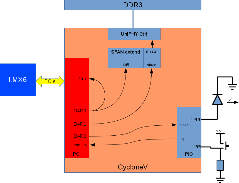
This is the full howto to make an APF6_SP CycloneV example design to use :
- PCIe
- DDR3
- LED
- Button
This howto is designed for :
- APF6D_SP-M1GE4G-4m-BW-C4M384: APF6_SP Dual with CycloneV C4 (speed C8) and two DDR3 chips
- Quartus 15.1.1 : Quartus 15 with update 1
To install quartus 15 see this page.
Make the quartus project
- Open the new project wizard in Quartus
- Select a directory for the design:
~/tmp/apf6_the_full_howto
- Open an empty project
- Change the device : right click on "Cyclone V"->Devices... in Project Navigator
- Select the part number : 5CGXFC4C7U19C8 then Ok
Make the Qsys project
- Open Qsys: Tools->Qsys
- Delete the component clk_0 then save the Qsys project with name : qsys_tfht.qsys
- Clic on finish and generate the component with all options left by default
- Under Quartus project add the Qsys project (don't forget to click on add after selected here.
- Right click on qsys_tfht.qsys and set as Top-Level Entity
- Relaunch Qsys by double-click on the file in project navigator
Adding the PCIe and CvP
- In IP Catalog select the component:
Library
    Interface Protocols
        PCI Express
            Avalon-MM Cyclone V Hard IP for PCI Express
- PCIe configuration:
- Number of Lanes: x1
- Reference clock frequency: 125Mhz
- check "Use 62.5 MHz application clock"
- BAR0: 32-bit non-prefetchable memory
- BAR1: 32-bit non-prefetchable memory
- BAR2: 32-bit non-prefetchable memory
- Vendor ID: 0x00001172
- Device ID: 0x0000e001
- Class Code: 0x00001300: there is a bug in quartus, the actual class code is here 13
- click on finish
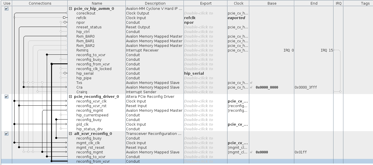
- Export these signal with name in bold:
- refclk : refclk
- npor: npor
- hip_serial: hip_serial
- connect Rxm_BAR0 on Cra
- Adding CvP component reconfig driver, with all default parameters:
Library
    Interface Protocols
        PCI Express
            Altera PCIe Reconfig Driver
- Connect these signals:
- coreclkout -> reconfig_xcvr_clk
- coreclkout -> pld_clk
- nreset_status -> reconfig_xcvr_rst
- Adding CvP component transceiver, with all default parameters:
Library
    Interface Protocols
        Transceiver PHY
            Transceiver Reconfiguration Controller
- Connect these signals:
- coreclkout -> mgmt_clk_clk
- nreset_status -> mgmt_rst_reset
- reconfig_mgmt -> reconfig_mgmt
- reconfig_driver.reconfig_busy -> reconfig_busy
- pci.reconfig_to_xcvr -> reconfig_to_xcvr
- pci.reconfig_from_xcvr -> reconfig_from_xcvr
Adding the DDR3
UniPHY controller
- In the IP catalog, select:
Library
    Memory Interfaces and Controllers
        Memory Interfaces with UniPHY
            DDR3 SDRAM Controller with UniPHY
- Select checkbox Enable Hard External Memory Interface
- In tab PHY Settings configure:
- Speed Grade: 8
- Memory clock frequency: 375Mhz
- PLL reference clock frequency: 62.5Mhz
- Rate on Avalon-MM interface: Full
- supply Voltage: 1.35V DDR3L
- In tab Memory Parameters
- In preset select: JEDEC DDR3-1G6 2GB X8 and apply
- Memory device speed grade: 400Mhz
- Total interface width: 24
- Row address width: 14
- In tab Controller Settings
- checkbox: Generate power-of-2 data bus widths for Qsys or SOPC Builder
- checkbox: Enable Configuration and Status Register Interface (Internacl JTAG)
- checkbox: Enable Error Detection and Correction Logic
- Click on finish
- Connect following signals:
- coreclkout -> pll_ref_clk
- coreclkout -> mp_cmd_clk_0
- coreclkout -> mp_rfifo_clk_0
- coreclkout -> mp_wfifo_clk_0
- coreclkout -> csr_clk
- nreset_status -> global_reset
- nreset_status -> soft_reset
- nreset_status -> mp_cmd_reset_n_0
- nreset_status -> mp_rfifo_reset_n_0
- nreset_status -> mp_wfifo_reset_n_0
- nreset_status -> csr_reset_n
Span extender
DDR3 memory is to large for PCIe BAR domain. Then we have to use a span extender to adapt PCIe BAR domain to DDR3 domain.
- Select span expander in IP Library:
Library
    Basic Functions
        Bridges and Adaptors
            Memory Mapped
                Address Span Extender
- Configure it with these options:
- Datapath Width: 64bits
- Slave Word Address Width: 20bits
- Finish
- Connect following extender signals:
- coreclckout -> clock
- nreset_status -> reset
- Rxm_BAR1 -> windowed_slave
- expanded_master -> avl_0
- Rxm_BAR0 -> cntl
- Change base address of cntl to 0x0000_4000
Adding the button and led (PIO)
- In IP Library select:
Library
    Processors and Peripherals
        Peripherals
            PIO (Parallel I/O)
- Configure it with these options:
- Direction: Bidir
- checkbox Synchronously capture
- Edge Type: RISING
- checkbox Generate IRQ
- IRQ Type: EDGE
- click on finish
- export external_connection to pio
- Connect following signals:
- coreclkout -> clk
- nreset_status -> reset
- Rxm_BAR2 -> s1
- irq -> Rxmirq
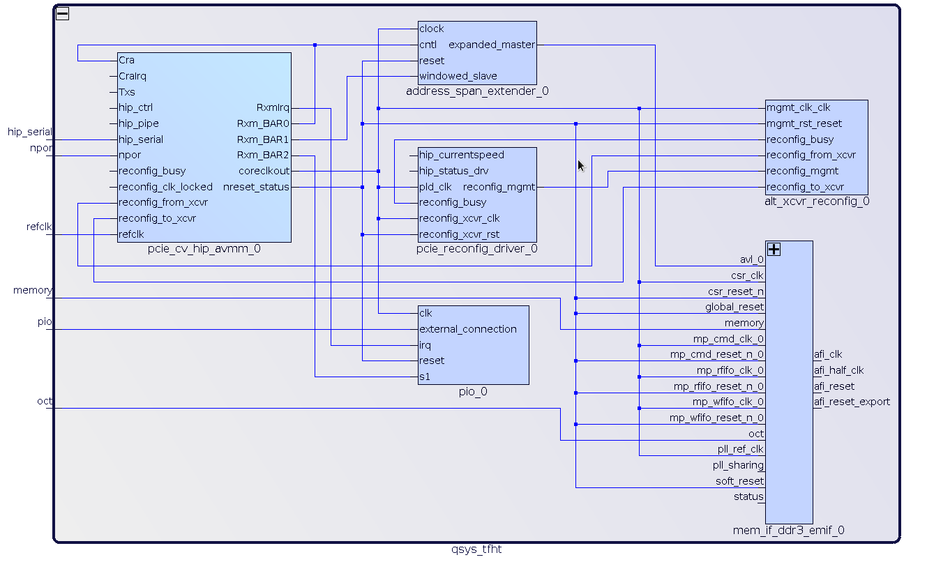
Qsys component schematic
The resulting schematics should give the figure below.
Now click on finish and generate the component with all default parameters kept.
Back to quartus project configuration
- Make a first synthesis, under task right click and start on :
Compile Design
    + Analysis & Synthesis
Pinout
- PCIe
- Create a file named 'pcie_pinout.tcl and edit it.
- Copy all lines from here.
- Save then add the file to project
- Run the script with following menu, select it then run:
Tools
    TCL Scripts ...
- DDR3
- Create a file named 'ddr3_pinout.tcl and edit it.
- Copy all lines from here (Pinout placement and Technology pinout).
- Save then add the file to project
- Run the script with following menu, select it then run:
Tools
    TCL Scripts ...
- Button & Led
Conclusion
This tutorial should give you the basics to use the CycloneV soldered on the APF6_SP module. Now you should know:
- PCIe:
- How to instanciate the CycloneV hard IP
- How to read/write data with it from Linux with simple access
- How to raise IRQ and transmit it to Linux
- DDR3:
- How to instanciate and configure the UniPHY hard IP
- How to connect it to PCIe
- How to read/write simple data
- Simple I/O:
- How to instanciate a simple port for I/O under Qsys
- How to drive it from Linux
Some subjects are not covered by this tutorial:
- Increase data bandwidth with PCIe-DMA (up to 140MB/s)
- From the FPGA to the i.MX6
- From the i.MX6 to the FPGA
- Create a custom Qsys component
- Using Serializer/Deserializer
- And more ...
If you are interested in a specific subject, please contact Armadeus System they should do somethings for you.


