APF6 SP The full howto
Contents
Introduction
This is the full howto make an APF6_SP CycloneV example design which uses :
- PCIe
- DDR3
- General Purpose Input/Outputs
- LED
- Button
This howto is designed for :
- APF6D_SP-M1GE4G-4m-BW-C4M384: APF6_SP Dual with CycloneV C4 (speed C8) and two DDR3 chips
- Quartus 15.1.1 : Quartus 15 with update 1
- To install Quartus 15 see this page.
Make the quartus project
- Open the "New Project Wizard" in Quartus
- Select a directory for the design, for example /home/your_name/workspace and a project name apf6_the_full_howto:
- Then Choose Empty Project and don't add any file yet -> press "Finish"
- Change the device : right click on "Cyclone V"->Devices... in Project Navigator
- Select the part number : 5CGXFC4C7U19C8
- In the same window, click on Device and Pin Options
- in CvP Settings set this options:
- Configuration via Protocol: Core initialization and update
- then select "OK" two times
Make the Qsys project
- Open Qsys: Tools->Qsys
- Delete the component clk_0 then save the Qsys project as : qsys_tfht.qsys
- Click on Finish and generate the component with all options left by default
- Under Quartus project add the Qsys project (don't forget to click on add after selected here).
- Right click on qsys_tfht.qsys and set as Top-Level Entity
- Relaunch Qsys by double-clicking on the file in "Project Navigator"
Adding the PCIe and CvP
- In IP Catalog select the component:
Library
    Interface Protocols
        PCI Express
            Avalon-MM Cyclone V Hard IP for PCI Express
- "Add" it to design.
- PCIe configuration:
- Number of Lanes: x1
- Reference clock frequency: 125Mhz
- check Use 62.5 MHz application clock
- check Enable configuration via the PCIe link
- BAR0: 32-bit non-prefetchable memory
- BAR1: 32-bit non-prefetchable memory
- BAR2: 32-bit non-prefetchable memory
- Vendor ID: 0x00001172
- Device ID: 0x0000e001
- Class Code: 0x00001300: there is a bug in quartus, the actual class code is here 13
- click on "Finish"
- Export these signals with name in bold (right click in "Hierarchy", then choose "Connections" and "Export as:...":
- refclk : refclk
- npor: npor
- hip_serial: hip_serial
- connect Rxm_BAR0 on Cra (always right click in "Hierarchy", then "Connections"...)
- Add CvP component reconfig driver, with all default parameters:
Library
    Interface Protocols
        PCI Express
            Altera PCIe Reconfig Driver
- Connect previous IP signals with:
- coreclkout -> reconfig_xcvr_clk
- coreclkout -> pld_clk
- nreset_status -> reconfig_xcvr_rst
- Add CvP component transceiver, with all default parameters:
Library
    Interface Protocols
        Transceiver PHY
            Transceiver Reconfiguration Controller
- Connect previous PCIe IP signals with:
- coreclkout -> mgmt_clk_clk
- nreset_status -> mgmt_rst_reset
- reconfig_mgmt -> reconfig_mgmt
- reconfig_driver.reconfig_busy -> reconfig_busy
- pci.reconfig_to_xcvr -> reconfig_to_xcvr
- pci.reconfig_from_xcvr -> reconfig_from_xcvr
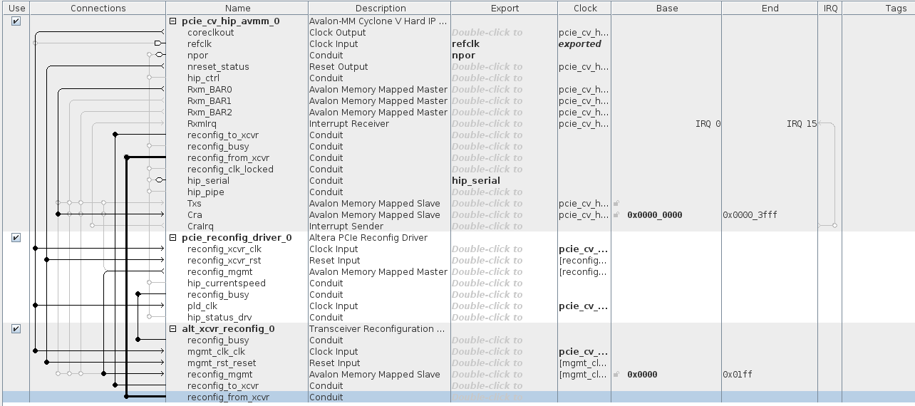
- you should end up with the following wiring:
Adding the DDR3
UniPHY controller
- In the IP catalog, select:
Library
    Memory Interfaces and Controllers
        Memory Interfaces with UniPHY
            DDR3 SDRAM Controller with UniPHY
- Select checkbox Enable Hard External Memory Interface
- In tab PHY Settings configure:
- Speed Grade: 8
- Memory clock frequency: 375Mhz
- PLL reference clock frequency: 62.5Mhz
- Rate on Avalon-MM interface: Full
- supply Voltage: 1.35V DDR3L
- In tab Memory Parameters
- In "Presets" (right of the window) select: JEDEC DDR3-1G6 2GB X8 and apply
- Memory device speed grade: 400Mhz
- Total interface width: 24
- Row address width: 14
- In tab Controller Settings
- checkbox: Generate power-of-2 data bus widths for Qsys or SOPC Builder
- checkbox: Enable Configuration and Status Register Interface (Internal JTAG)
- checkbox: Enable Error Detection and Correction Logic
- Click on Finish
- Connect following signals:
- coreclkout -> pll_ref_clk
- coreclkout -> mp_cmd_clk_0
- coreclkout -> mp_rfifo_clk_0
- coreclkout -> mp_wfifo_clk_0
- coreclkout -> csr_clk
- nreset_status -> global_reset
- nreset_status -> soft_reset
- nreset_status -> mp_cmd_reset_n_0
- nreset_status -> mp_rfifo_reset_n_0
- nreset_status -> mp_wfifo_reset_n_0
- nreset_status -> csr_reset_n
Span extender
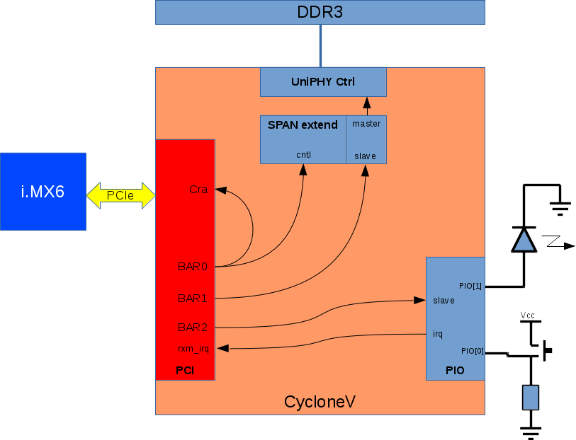
DDR3 memory is to large for PCIe BAR domain. Then we have to use a span extender to adapt PCIe BAR domain to DDR3 domain.
- Select span expander in IP Library:
Library
    Basic Functions
        Bridges and Adaptors
            Memory Mapped
                Address Span Extender
- Configure it with these options:
- Datapath Width: 64bits
- Slave Word Address Width: 20bits
- press "Finish"
- Connect following extender signals:
- coreclckout -> clock
- nreset_status -> reset
- Rxm_BAR1 -> windowed_slave
- expanded_master -> avl_0
- Rxm_BAR0 -> cntl
- Change base address of cntl to 0x0000_4000
Adding the button and led (PIO)
Documentation of the PIO component can be found here.
- In IP Library select:
Library
    Processors and Peripherals
        Peripherals
            PIO (Parallel I/O)
- Configure it with these options:
- Width: 2
- Direction: Bidir
- checkbox Synchronously capture
- Edge Type: RISING
- checkbox Generate IRQ
- IRQ Type: EDGE
- click on finish
- export external_connection to pio
- Connect following signals:
- coreclkout -> clk
- nreset_status -> reset
- Rxm_BAR2 -> s1
- irq -> Rxmirq
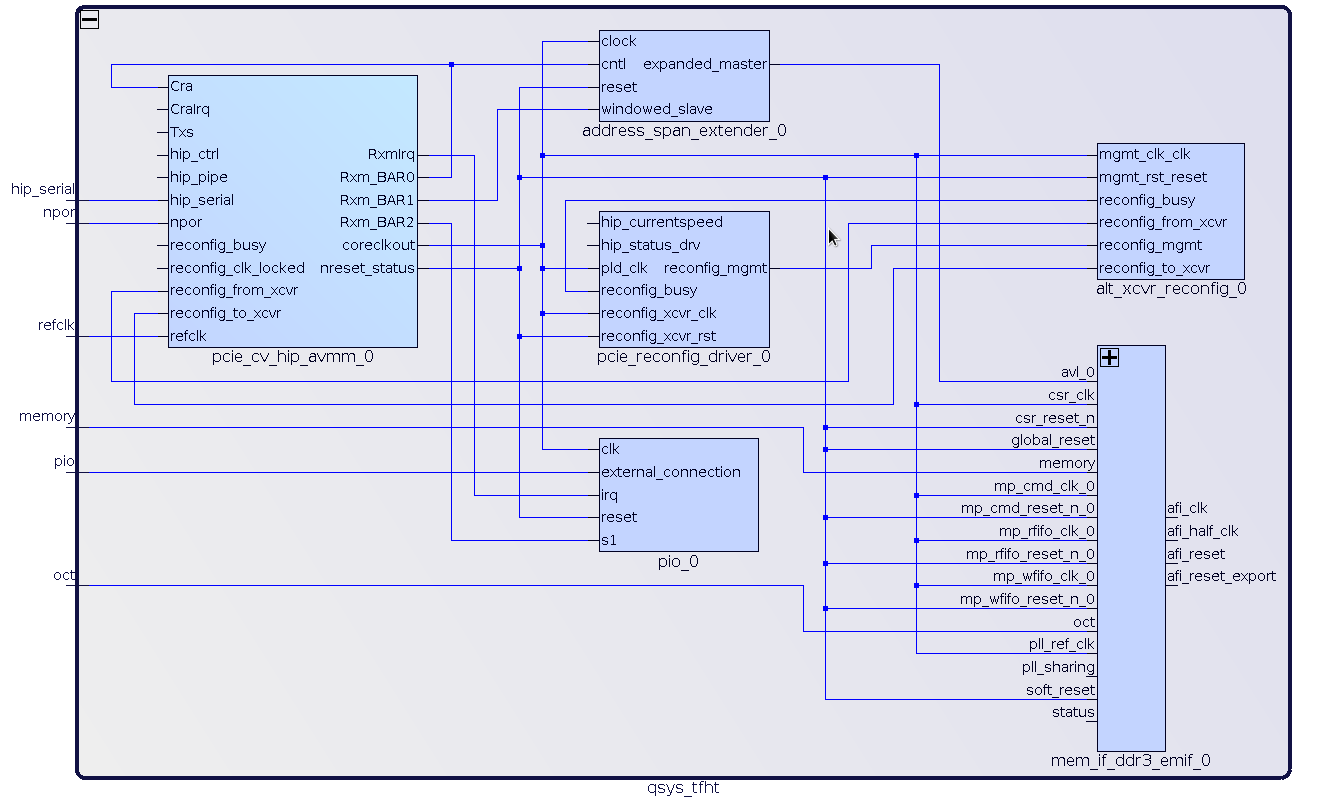
Qsys component schematic
The resulting schematics should give the figure below.
Now click on finish and generate the component with all default parameters kept.
Generate bitstream with Quartus
- Make a first synthesis, under task right click and start on :
Compile Design
    + Analysis & Synthesis
Pinout
- PCIe
- Create a file named 'pcie_pinout.tcl and edit it.
- Copy all lines from here.
- Save then add the file to project
- Run the script with following menu, select it then run:
Tools
    TCL Scripts ...
- DDR3
- Create a file named 'ddr3_pinout.tcl and edit it.
- Copy all lines from here (Pinout placement and Technology pinout).
- Save then add the file to project
- Run the script with following menu, select it then run:
Tools
    TCL Scripts ...
- Button & Led
- Open the pinplanner by double-click in tasks:
Compile Design
    Analysis & Synthesis
        I/O Assignment Analysis
            Pin Planner
- For button pio_export[0] select Location column and set it to : PIN_L9
- For led pio_export[1] select Location column and set it to : PIN_M10
- Close the Pin Planner
Synthesis, Place & route
- Right click on Analysis and Synthesis then Start
- Open a Linux console terminal then go to your project directory and type this:
$ cd ~/tmp/apf6_the_full_howto
$ find . -name "*_p0_pin_map.tcl" | xargs sed -iolt "/_mem_if_ddr3_emif_0_p0_get_input_clk_id {/a     return \$pll_output_node_id"
- Right click on Assembler (Generate programming files) then Start
- Convert bitstream to rbf with menu:
File
   Convert Programming Files...
- set these options:
- Programming file type: Raw Binary File (.rbf)
- Change the name to : output_files/tfht.rbf
- Select SOF Data in Input files to convert then click on Add File...
- add the file apf6_the_full_howto.sof in directory output_files
- checkbox Create CvP files (Generate tfht.periph.rbf and tfht.core.rbf)
- click on Generate
- These files should be present on directory output_files:
ls -l tmp/apf6_the_full_howto/output_files/*.rbf
tmp/apf6_the_full_howto/output_files/tfht.core.rbf
tmp/apf6_the_full_howto/output_files/tfht.periph.rbf
Linux BSP configuration
| |
Note: This is not an Armadeus BSP tutorial, the BSP is supposed to be installed and compiled according to this explains |
- Get a compiled BSP with following configuration : apf6_defconfig
- Add PCI debug package with make menuconfig
Target packages  --->
    Hardware handling  --->
        [*] pcidebug
$ cp -v output_files/tfht.*.rbf /tftpboot/
‘output_files/tfht.core.rbf’ -> ‘/tftpboot/tfht.core.rbf’
‘output_files/tfht.periph.rbf’ -> ‘/tftpboot/tfht.periph.rbf’
| |
Note: Refer to PCIe FPGA loading to understand FPGA configuration with PCIe |
- In U-Boot download the periph.rbf and configure FPGA (don't forget to configure your tftp server ip):
BIOS> tftpboot ${loadaddr} 192.168.0.214:tfht.periph.rbf
BIOS> fpga load 0 ${loadaddr} ${filesize}
- Boot Linux
BIOS> boot
...
apf6 login: root
- The three BARx should be seen with lspci command :
# lspci -v -s 01:00.0
01:00.0 Unclassified device [0013]: Altera Corporation Device e001 (rev 01)
        Flags: fast devsel, IRQ 341
        Memory at 01800000 (32-bit, non-prefetchable) [disabled] [size=32K]
        Memory at 01000000 (32-bit, non-prefetchable) [disabled] [size=8M]
        Memory at 01808000 (32-bit, non-prefetchable) [disabled] [size=32]
        Capabilities: [50] MSI: Enable- Count=1/4 Maskable- 64bit+
        Capabilities: [78] Power Management version 3
        Capabilities: [80] Express Endpoint, MSI 00
        Capabilities: [100] Virtual Channel
        Capabilities: [200] Vendor Specific Information: ID=1172 Rev=0 Len=044 <?>
- Configure network:
$ udhcpc
- Download core:
$ tftp -g -r tfht.core.rbf 192.168.0.214
- Load the core bitstream:
$ load_fpga tfht.core.rbf
Altera CvP 0000:01:00.0: enabling device (0140 -> 0142)
Altera CvP 0000:01:00.0: Found and enabled PCI device with VID 0x1172, DID 0xE001
successfully init Altera CVP with major 248
Altera CvP 0000:01:00.0: Now starting CvP...
Altera CvP 0000:01:00.0: CvP successful, application layer now ready
8212+1 records in
8212+1 records out
User access to FPGA
DDR3
- DDR3 is accessible via the BAR1, connect to BAR1:
$ pci_debug -s 01:00.0 -b1
- Read first values of DDR3:
PCI> d32 0 20

00000000: AAAAAAAA AAAAAAAA AAAAAAAA AAAAAAAA
00000010: 55555555 55555555 55555555 55555555
- Write values, then read back:
PCI> c32 0 CAFEDECA
PCI> c32 8 CACABEBE
PCI> d32 0 20

00000000: CAFEDECA AAAAAAAA CACABEBE AAAAAAAA
00000010: 55555555 55555555 55555555 55555555
- Exit pci_debug
PCI> quit
Only first 8MB (0x800000) are accessible for the moment, to access next 8MB, the span extender must be configured on BAR0.
- Access BAR0 and configure span extender:
$ pci_debug -s 01:00.0 -b0
- Read the span extender windows value at address 0x4000:
PCI> d32 4000 1

00004000: 00000000
- Write the new required value :
PCI> c32 4000 800000
PCI> d32 4000 1

00004000: 00800000
- Quit then reconnect pci_debug to change for bar1:
PCI> quit
$ pci_debug -s 01:00.0 -b1
- Read value :
PCI> d32 0 20

00000000: 6B2171EA DFA5DA76 6CFB3F47 7AF9F526
00000010: DBD85BAB 7F56CF7A 78FAD73B ECF997FE
- Write some values:
PCI> c32 0 12345678
PCI> c32 4 9ABCDEF0
PCI> c32 10 12345678
PCI> c32 14 9ABCDEF0
PCI> d32 0 20

00000000: 12345678 9ABCDEF0 6CFB3F47 7AF9F526
00000010: 12345678 9ABCDEF0 78FAD73B ECF997FE
- Etc...
PIO (Button and led)
As seen on the first schematic of this tutorial, the PIO is plugged on the BAR2 of the PCIe.
- Then first, connect to BAR2 with pci_debug:
$ pci_debug -s 01:00.0 -b2
Button
- Read all PIO registers:
PCI> d32 0 8

00000000: 00000001 00000000
- Leave button pressed and read again:
PCI> d32 0 8

00000000: 00000000 00000000
led
- set PIO[1] (led) as output:
PCI> c32 4 2
- Turn on led
PCI> c32 0 2
- Turn off led:
PCI> c32 0 0
Conclusion
This tutorial should give you the basics to use the CycloneV soldered on the APF6_SP module. Now you should know:
- PCIe:
- How to instanciate the CycloneV hard IP
- How to read/write data with it from Linux with simple access
- DDR3:
- How to instanciate and configure the UniPHY hard IP
- How to connect it to PCIe
- How to read/write simple data
- Simple I/O:
- How to instanciate a simple port for I/O under Qsys
- How to drive it from Linux
Some subjects are not covered by this tutorial:
- Managing PCIe interrupts
- Write a Linux driver
- Increase data bandwidth with PCIe-DMA (up to 140MB/s)
- From the FPGA to the i.MX6
- From the i.MX6 to the FPGA
- Create a custom Qsys component
- Using Serializer/Deserializer
- And more ...
If you are interested in a specific subject, please contact Armadeus System they should do somethings for you.


