Difference between revisions of "APF27 FPGA-IMX interface description"
From ArmadeusWiki
m (New page: This article describe the interface between IMX and SPARTAN3A on APF27. == Hardware == == Timings configuration == == Firmware (FPGA)== == Software ==) |
|||
| Line 1: | Line 1: | ||
| − | This article describe the interface between IMX and | + | This article describe the interface between IMX and Spartan3A on APF27. |
| + | Documentation of i.MX interface can be found in [http://TODO reference manual] chapter 17 | ||
| + | «Wireless External Interface Module (WEIM)». | ||
== Hardware == | == Hardware == | ||
| + | |||
| + | Electronic schematic of apf27 fpga interface can be found on | ||
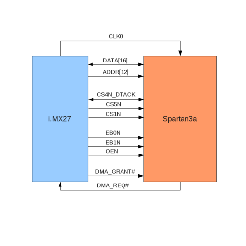
| + | [http://www.armadeus.com/_downloads/apf27/hardware/apf27_V1.2.pdf this document] page 11. Simplified schema is describe bellow on figure 1. | ||
| + | |||
| + | [[image:fpgaimx_wire.png|center|500px|thumb|'''figure 1''' - ''FPGA-i.MXL wiring'']] | ||
| + | |||
| + | Signals used in design are : | ||
| + | |||
| + | * '''CLKO''' : Clock generated by i.MX used as general clock by the fpga. | ||
| + | * '''DATA[16]''' : 16 bits data bus. | ||
| + | * '''ADDR[13]''' : 12 bits data bus, least significant bit (ADDR[0]) is not used because only word access are done. | ||
| + | * '''CS4N_DTACK''': '''C'''hip '''S'''elect 4 or '''D'''ata '''T'''ransmit '''ACK'''nowledge. | ||
| + | * '''CS5''','''CS1''' : '''C'''hip '''S'''elect 5 and 1. | ||
| + | * '''EB0N''' and '''EB1N''': For '''E'''nable '''B'''yte, write signal for lower byte and upper byte on data bus. | ||
| + | * '''OEN''' : For '''O'''utput '''E'''nable bit, read signal. | ||
| + | * '''DMA_GRANT#''' and '''DMA_REQ#''' : Signals to use DMA on i.MX. | ||
| + | |||
== Timings configuration == | == Timings configuration == | ||
== Firmware (FPGA)== | == Firmware (FPGA)== | ||
== Software == | == Software == | ||
Revision as of 12:01, 31 July 2009
This article describe the interface between IMX and Spartan3A on APF27. Documentation of i.MX interface can be found in reference manual chapter 17 «Wireless External Interface Module (WEIM)».
Hardware
Electronic schematic of apf27 fpga interface can be found on this document page 11. Simplified schema is describe bellow on figure 1.
Signals used in design are :
- CLKO : Clock generated by i.MX used as general clock by the fpga.
- DATA[16] : 16 bits data bus.
- ADDR[13] : 12 bits data bus, least significant bit (ADDR[0]) is not used because only word access are done.
- CS4N_DTACK: Chip Select 4 or Data Transmit ACKnowledge.
- CS5,CS1 : Chip Select 5 and 1.
- EB0N and EB1N: For Enable Byte, write signal for lower byte and upper byte on data bus.
- OEN : For Output Enable bit, read signal.
- DMA_GRANT# and DMA_REQ# : Signals to use DMA on i.MX.
