Difference between revisions of "APF27 FPGA-IMX interface description"
m |
|||
| Line 1: | Line 1: | ||
This article describe the interface between IMX and Spartan3A on APF27. | This article describe the interface between IMX and Spartan3A on APF27. | ||
Documentation of i.MX interface can be found in [http://TODO reference manual] chapter 17 | Documentation of i.MX interface can be found in [http://TODO reference manual] chapter 17 | ||
| − | «Wireless External Interface Module (WEIM)». | + | «Wireless External Interface Module ('''WEIM''')». |
== Hardware == | == Hardware == | ||
| Line 29: | Line 29: | ||
== Chip Select Timings configuration == | == Chip Select Timings configuration == | ||
| + | ===Present configuration (static timing)=== | ||
Present configuration use '''CS5''' for accessing FPGA. 32 bits register CS5 | Present configuration use '''CS5''' for accessing FPGA. 32 bits register CS5 | ||
is used to configure all timing for this chip select. It's default | is used to configure all timing for this chip select. It's default | ||
| Line 36: | Line 37: | ||
State Control). | State Control). | ||
* CS5L (Lower 16bits,see page 525 of reference manual) : mw D8002054 00000D01 | * CS5L (Lower 16bits,see page 525 of reference manual) : mw D8002054 00000D01 | ||
| − | Enable chip select (CSEN), Enable EB[] (EBC) and select data port size to | + | Enable chip select (CSEN), Enable for only write access EB[] (EBC) and select data port size to |
16bits (DSZ : Data port SiZe). | 16bits (DSZ : Data port SiZe). | ||
* CS5A (additionnal register, page 528) : mw D8002058 0 | * CS5A (additionnal register, page 528) : mw D8002058 0 | ||
| + | |||
| + | * WCR (WEIM Configuration Register) : mw D8002060 00002000 | ||
| + | Address unshifted for CS5 (AUS5) | ||
| + | |||
| + | [[image:timingstatic.png|center|500px|thumb|'''figure 2''' - ''Static timings chronograms'']] | ||
| + | |||
| + | With this configuration, acces time (read/write) to fpga is garanted to 50ns. | ||
| + | |||
| + | This configuration is interesting because all timings are under control. But | ||
| + | the problem is that to be perfectly synchronous, fpga is clocked at 133MHz | ||
| + | like WEIM and some IP design doesn't work at this frequency. | ||
| + | |||
| + | To solve the problem, a solution can be to divide by 2 CLKO clock frequency. But | ||
| + | it's relatively low and access time must be extend. | ||
| + | |||
| + | ===Futur configuration (with DTACK)=== | ||
| + | |||
| + | To solve above problem, another solution can be the DTACK signal. DTACK signal | ||
| + | is emmited by slave to master when write/read is done. | ||
| + | With this solution, access time is variable and their no need to define | ||
| + | timings. | ||
| + | |||
| + | |||
== Firmware (FPGA)== | == Firmware (FPGA)== | ||
Revision as of 16:56, 31 July 2009
This article describe the interface between IMX and Spartan3A on APF27. Documentation of i.MX interface can be found in reference manual chapter 17 «Wireless External Interface Module (WEIM)».
Contents
Hardware
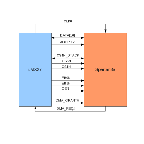
Electronic schematic of apf27 fpga interface can be found on this document page 11. Simplified schema is describe bellow on figure 1.
Signals used in design are :
- CLKO : Clock generated by i.MX used as general clock by the fpga.
- DATA[16] : 16 bits data bus.
- ADDR[13] : 12 bits data bus, least significant bit (ADDR[0]) is not used because only word access are done.
- CS4N_DTACK: Chip Select 4 or Data Transmit ACKnowledge.
- CS5,CS1 : Chip Select 5 and 1.
- EB0N and EB1N: For Enable Byte, write signal for lower byte and upper byte on data bus.
- OEN : For Output Enable bit, read signal.
- DMA_GRANT# and DMA_REQ# : Signals to use DMA on i.MX.
Each chip select has its own configuration that can be use for slave that have differents timings.
CLKO is configured at 133MHz to be synchronous with WEIM bus that is internally clocked at 133MHz too.
Chip Select Timings configuration
Present configuration (static timing)
Present configuration use CS5 for accessing FPGA. 32 bits register CS5 is used to configure all timing for this chip select. It's default configuration is :
- CS5U (Upper 16bits,see page 521 of reference manual ) : mw D8002050 00000600
This will add 6 waits state on access to read value correctly (WSC : Wait State Control).
- CS5L (Lower 16bits,see page 525 of reference manual) : mw D8002054 00000D01
Enable chip select (CSEN), Enable for only write access EB[] (EBC) and select data port size to 16bits (DSZ : Data port SiZe).
- CS5A (additionnal register, page 528) : mw D8002058 0
- WCR (WEIM Configuration Register) : mw D8002060 00002000
Address unshifted for CS5 (AUS5)
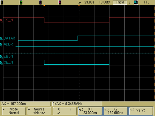
With this configuration, acces time (read/write) to fpga is garanted to 50ns.
This configuration is interesting because all timings are under control. But the problem is that to be perfectly synchronous, fpga is clocked at 133MHz like WEIM and some IP design doesn't work at this frequency.
To solve the problem, a solution can be to divide by 2 CLKO clock frequency. But it's relatively low and access time must be extend.
Futur configuration (with DTACK)
To solve above problem, another solution can be the DTACK signal. DTACK signal is emmited by slave to master when write/read is done. With this solution, access time is variable and their no need to define timings.
Firmware (FPGA)
Software
All registers configuration for external memory are done in u-boot. Configuration file can be found in buildroot/project_build_armv5te/<project_name>/u-boot-1.3.4/include/configs/apf27.h And is saved in armadeus tree at buildroot/target/device/armadeus/apf27/apf27.h

