Difference between revisions of "IMX27-Spartan3A interface description"
From ArmadeusWiki
| Line 3: | Line 3: | ||
[[image:Imx27-spartan3A.jpg|700px|center|thumb|'''figure 1''' - ''i.MX27-Spartan3A bus description'']] | [[image:Imx27-spartan3A.jpg|700px|center|thumb|'''figure 1''' - ''i.MX27-Spartan3A bus description'']] | ||
| − | All signals plugged between I.MX27 and spartan3A are described on figure 1. Some others signals are used only for fpga configuration. For more informations about the FPGA wiring, see the [[Datasheet#APF27 | APF27 schematics]] and the [http://cache.freescale.com/files/32bit/doc/ref_manual/MCIMX27RM.pdf?fsrch=1&WT_TYPE=Reference%20Manuals&WT_VENDOR=FREESCALE&WT_FILE_FORMAT=pdf&WT_ASSET=Documentation&sr=2 i.MX27 reference manual], especially the WEIM chapter. | + | All signals plugged between I.MX27 and spartan3A are described on figure 1: |
| + | |||
| + | * CLKO: Clock generated by i.MX. Used as general clock by the FPGA. | ||
| + | * DATA[15:0]: Data bus. | ||
| + | * ADDR[12:1]: Address bus. All access are down in 16bits, then pin 0 is not used and not plugged. | ||
| + | * CS4N_DTACK: Chip select 4 (0xD400_0000 to 0xD5FF_FFFF ) or Data Transmit ACKnowledge. This signal can be used as DTACK for asynchronous access with chip select 5. | ||
| + | * CS5N: Chip select 5 (0xD600_0000 to 0xD7FF_FFFF ). | ||
| + | * CS1N: Chip select 1 (0xC800_0000 to 0xCFFF_FFFF ). | ||
| + | * EB0N, EB1N: For Enable Byte, write signal for lower byte and upper byte on data bus. | ||
| + | * OEN: For Output Enable bit, read signal. | ||
| + | * DMA_GRANT#: Signals to use DMA on i.MX. | ||
| + | * DMA_REQ#: Signals to use DMA on i.MX. | ||
| + | |||
| + | |||
| + | Some others signals are used only for fpga configuration. For more informations about the FPGA wiring, see the [[Datasheet#APF27 | APF27 schematics]] and the [http://cache.freescale.com/files/32bit/doc/ref_manual/MCIMX27RM.pdf?fsrch=1&WT_TYPE=Reference%20Manuals&WT_VENDOR=FREESCALE&WT_FILE_FORMAT=pdf&WT_ASSET=Documentation&sr=2 i.MX27 reference manual], especially the WEIM chapter. | ||
Revision as of 17:06, 12 January 2012
This article describe the bus interface configuration to communicate between i.MX27 processor and Spartan3A FPGA.
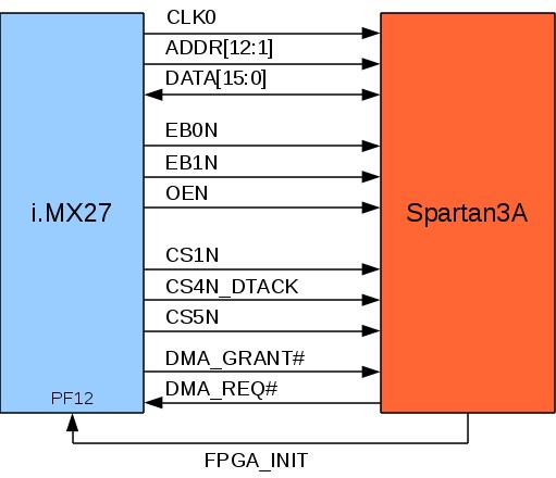
All signals plugged between I.MX27 and spartan3A are described on figure 1:
- CLKO: Clock generated by i.MX. Used as general clock by the FPGA.
- DATA[15:0]: Data bus.
- ADDR[12:1]: Address bus. All access are down in 16bits, then pin 0 is not used and not plugged.
- CS4N_DTACK: Chip select 4 (0xD400_0000 to 0xD5FF_FFFF ) or Data Transmit ACKnowledge. This signal can be used as DTACK for asynchronous access with chip select 5.
- CS5N: Chip select 5 (0xD600_0000 to 0xD7FF_FFFF ).
- CS1N: Chip select 1 (0xC800_0000 to 0xCFFF_FFFF ).
- EB0N, EB1N: For Enable Byte, write signal for lower byte and upper byte on data bus.
- OEN: For Output Enable bit, read signal.
- DMA_GRANT#: Signals to use DMA on i.MX.
- DMA_REQ#: Signals to use DMA on i.MX.
Some others signals are used only for fpga configuration. For more informations about the FPGA wiring, see the APF27 schematics and the i.MX27 reference manual, especially the WEIM chapter.
