Difference between revisions of "IMX27-Spartan3A interface description"
| Line 75: | Line 75: | ||
By default, the wishbone bus is proposed on the spartan3A fpga. A WEIM to Wishbone wrapper is used, which is available under POD default libraries in wrappers lib. The component is named imx27_wb16_wrapper. | By default, the wishbone bus is proposed on the spartan3A fpga. A WEIM to Wishbone wrapper is used, which is available under POD default libraries in wrappers lib. The component is named imx27_wb16_wrapper. | ||
| + | |||
| + | |||
== The FPGA interrupt == | == The FPGA interrupt == | ||
| Line 81: | Line 83: | ||
Note : With default apf27 kernel 2.6.29.x the GPIOlib can use interrupt event, but can't configure it with ''/sys/class/gpio/gpio172/edge'' file. Interrupt must be configured under the kernel sources. The ''/sys/class/gpio/gpio172/edge'' file can be use only with [[APF9328_and_APF27_migration_to_Linux_2.6.36 | kernel 2.6.38.x]]. | Note : With default apf27 kernel 2.6.29.x the GPIOlib can use interrupt event, but can't configure it with ''/sys/class/gpio/gpio172/edge'' file. Interrupt must be configured under the kernel sources. The ''/sys/class/gpio/gpio172/edge'' file can be use only with [[APF9328_and_APF27_migration_to_Linux_2.6.36 | kernel 2.6.38.x]]. | ||
| + | |||
| + | == Pinout == | ||
| + | |||
| + | {| border="1" cellpadding="5" cellspacing="0" align="center" | ||
| + | |- style="background:#efefef;" align="center" | ||
| + | ! Schematic name !! i.MX27 gpio !! Spartan3A IO !! Spartan3A Ball !! Description | ||
| + | |- align="center" | ||
| + | | DATA[0] || - || IO_L06P_2/D7 || T5 || Data bus 0 | ||
| + | |- align="center" | ||
| + | | DATA[1] || - || IO_L06N_2/D6 || T6 || Data bus 1 | ||
| + | |- align="center" | ||
| + | | DATA[2] || - || IO_L08P_2/D5 || P7 || Data bus 2 | ||
| + | |- align="center" | ||
| + | | DATA[3] || - || IO_L08N_2/D4 || N8 || Data bus 3 | ||
| + | |- align="center" | ||
| + | | DATA[4] || - || IO_L17N_2/D3 || P12 || Data bus 4 | ||
| + | |- align="center" | ||
| + | | DATA[5] || - || IO_L18P_2/D2 || T13 || Data bus 5 | ||
| + | |- align="center" | ||
| + | | DATA[6] || - || IO_L18N_2/D1 || R13 || Data bus 6 | ||
| + | |- align="center" | ||
| + | | DATA[7] || - || IO_L20P_2/D0/DIN/MISO || T14 || Data bus 7 | ||
| + | |- align="center" | ||
| + | | DATA[8] || - || IO_L04N_2/VS0 || P5 || Data bus 8 | ||
| + | |- align="center" | ||
| + | | DATA[9] || - || IO_L04P_2/VS1 || N6 || Data bus 9 | ||
| + | |- align="center" | ||
| + | | DATA[10] || - || IO_L03N_2/VS2 || T3 || Data bus 10 | ||
| + | |- align="center" | ||
| + | | DATA[11] || - || IO_L15P_2/AWAKE || T11 || Data bus 11 | ||
| + | |- align="center" | ||
| + | | DATA[12] || - || IO_L05P_2 || T4 || Data bus 12 | ||
| + | |- align="center" | ||
| + | | DATA[13] || - || IO_L05N_2 || R5 || Data bus 13 | ||
| + | |- align="center" | ||
| + | | DATA[14] || - || IO_L13N_2 || M10 || Data bus 14 | ||
| + | |- align="center" | ||
| + | | DATA[15] || - || IO_L14P_2 || T10 || Data bus 15 | ||
| + | |- align="center" | ||
| + | |||
| + | | ADDR1 || - || IP_21/VREF_2 ||N5 || Address bus pin 1 | ||
| + | |- align="center" | ||
| + | | ADDR2 || - || IP_22 ||L7 || Address bus pin 2 | ||
| + | |- align="center" | ||
| + | | ADDR3 || - || IP_23/VREF_2 ||M7 || Address bus pin 3 | ||
| + | |- align="center" | ||
| + | | ADDR4 || - || IP_24/VREF_2 ||M8 || Address bus pin 4 | ||
| + | |- align="center" | ||
| + | | ADDR5 || - || IP_25 ||L8 || Address bus pin 5 | ||
| + | |- align="center" | ||
| + | | ADDR6 || - || IP_26/VREF_2 ||L9 || Address bus pin 6 | ||
| + | |- align="center" | ||
| + | | ADDR7 || - || IP_27/VREF_2 ||L10 || Address bus pin 7 | ||
| + | |- align="center" | ||
| + | | ADDR8 || - || IP_28/VREF_2 ||M11 || Address bus pin 8 | ||
| + | |- align="center" | ||
| + | | ADDR9 || - || IO_L16P_2 ||P11 || Address bus pin 9 | ||
| + | |- align="center" | ||
| + | | ADDR10 || - || IO_L16N_2 ||N11 || Address bus pin 10 | ||
| + | |- align="center" | ||
| + | | ADDR11 || - || IO_L19P_2 ||N12 || Address bus pin 11 | ||
| + | |- align="center" | ||
| + | | ADDR12 || - || IO_L19N_2 ||P13 || Address bus pin 12 | ||
| + | |- align="center" | ||
| + | | CS4N_DTACK || PF21 || IO_L03P_2/RDWR_B ||R3 || Chip select 4 | ||
| + | |- align="center" | ||
| + | | CS5N || PF22 ||IO_L14N_2/MOSI/CSI_B ||P10 || Chip select 5 | ||
| + | |- align="center" | ||
| + | | CS1N || - || IO_L10N_2/GCLK15 || T8 || Chip select 1 | ||
| + | |- align="center" | ||
| + | | EB0N || - || IO_L11N_2/GCLK1 || P9 || Enable Byte 0 | ||
| + | |- align="center" | ||
| + | | EB1N || - || IO_L10P_2/GCLK14 || P8 || Enable Byte 1 | ||
| + | |- align="center" | ||
| + | | OEN || - || IO_L12P_2/GCLK2 || R9 || Output Enable bit | ||
| + | |- align="center" | ||
| + | | DMA_GRANT# || PD27 || IO_L09P_2/GCLK12 || R7 || DMA access | ||
| + | |- align="center" | ||
| + | | DMA_REQ# || PD25 || IO_L12N_2/GCLK3 || T9 || DMA access | ||
| + | |- align="center" | ||
| + | | CLKO || PF15 || IO_L11P_2/GCLK0||N9 || Clock | ||
| + | |- align="center" | ||
| + | | FPGA_INIT || PF12 || IO_L17P_2/INIT_B || T12 || Used by default for interrupts | ||
| + | |||
| + | |} | ||
Revision as of 11:54, 23 January 2012
Contents
Introduction
This article describes the bus interface configuration to communicate between the i.MX27 processor and the Spartan3A FPGA of the APF27 board.
Simplified view
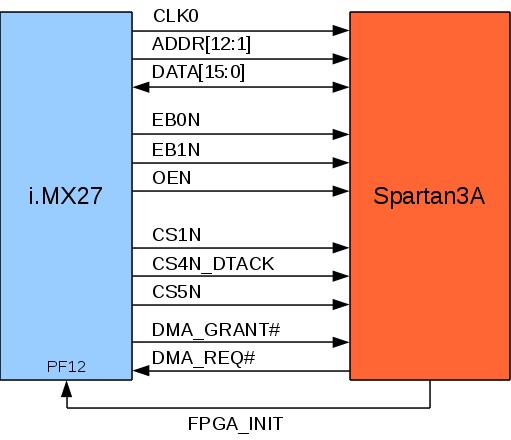
Figure 1 is a simplified view of apf27 schematics (page 11). Signals are :
- DATA[15:0]: Data bus.
- ADDR[12:1]: Address bus. All access are done in 16bits, this means that A0 is not used and not connected.
- CS4N_DTACK: Chip select 4 (0xD400_0000 to 0xD5FF_FFFF ) or Data Transmit ACKnowledge. This signal can be used as DTACK for asynchronous access with chip select 5.
- CS5N: Chip select 5 (0xD600_0000 to 0xD7FF_FFFF ). Chip select 5. Configured by default for FPGA communication.
- CS1N: Chip select 1 (0xC800_0000 to 0xCFFF_FFFF ). Chip select 1
- EB0N, EB1N: For Enable Byte, write signal for lower byte and upper byte on data bus.
- OEN: For Output Enable bit, read signal.
- DMA_GRANT#: Required for DMA access (future development).
- DMA_REQ#: Required for DMA access (future development)
Not part of WEIM bus :
- CLKO: Clock generated by the i.MX. Used as a general clock by the FPGA.
- FPGA_INIT: Not part of i.MX27 WEIM bus but used by default for interrupts (GPIO PF12).
Signals in bold are used in default configuration. Some others signals are used only for firmware download. For more informations about the FPGA wiring, see the APF27 schematics and the i.MX27 reference manual, especially the WEIM chapter.
Default configuration on CS5N
Clock
The clock used to clock the fpga is CLK0 and is configured to 100 MHz.
Chip select
By default the chip select 5 (CS5N) is used for communication. The address domain corresponding to this chip select can be found in i.MX27 reference manual in chapter 2 (Secondary AHB Port 2 Memory Map page 129).
| Start Address | End Address | Size | Region |
|---|---|---|---|
| 0xC800 0000 | 0xCFFF FFFF | 128M | WEIM External Memory (CS1) |
| 0xD400 0000 | 0xD5FF FFFF | 32M | WEIM External Memory (CS4) |
| 0xD600 0000 | 0xD7FF FFFF | 32M | WEIM External Memory (CS5) |
Other chip select (CS1 and CS4) can be used to extend the memory domain or to use different timing configuration with the same Address/Data bus signals. The default bus configuration for the APF27 can be found in the file apf27.h in u-boot sources : buildroot/target/device/armadeus/apf27/apf27-u-boot-1.3.4.h
Especially these lines :
/* FPGA 16 bit data bus */
#define CFG_CS5U_VAL	0x00000600
#define CFG_CS5L_VAL	0x00000D01
#define CFG_CS5A_VAL	0
| |
Note: Do not forget to do :
$ make u-boot-dirclean
$ make
To test your modification under the apf27-u-boot-1.3.4.h file |
It is not necessary to modify apf27.h file and recompile U-Boot for WEIM timings test, register can be read/written via U-Boot or Linux.
To access these register with U-Boot or Linux, use the address given under the reference manual in WEIM register descriptions (17.5.3 Register Descriptions).
Timings
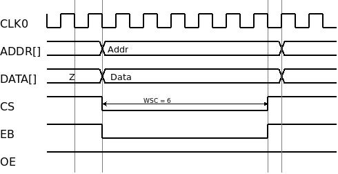
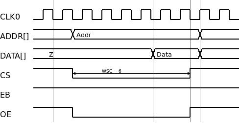
Following chronograms represent WEIM read and write configured for APF27.
FPGA side
By default, the wishbone bus is proposed on the spartan3A fpga. A WEIM to Wishbone wrapper is used, which is available under POD default libraries in wrappers lib. The component is named imx27_wb16_wrapper.
The FPGA interrupt
By default under POD the pin FPGA_INIT (PF12) is used for the interrupt manager irq_mngr. For simple user application the gpio can be used with the GPIOlib interface, the gpio number will then be (6-1)x32+12 = 172.
Note : With default apf27 kernel 2.6.29.x the GPIOlib can use interrupt event, but can't configure it with /sys/class/gpio/gpio172/edge file. Interrupt must be configured under the kernel sources. The /sys/class/gpio/gpio172/edge file can be use only with kernel 2.6.38.x.
Pinout
| Schematic name | i.MX27 gpio | Spartan3A IO | Spartan3A Ball | Description |
|---|---|---|---|---|
| DATA[0] | - | IO_L06P_2/D7 | T5 | Data bus 0 |
| DATA[1] | - | IO_L06N_2/D6 | T6 | Data bus 1 |
| DATA[2] | - | IO_L08P_2/D5 | P7 | Data bus 2 |
| DATA[3] | - | IO_L08N_2/D4 | N8 | Data bus 3 |
| DATA[4] | - | IO_L17N_2/D3 | P12 | Data bus 4 |
| DATA[5] | - | IO_L18P_2/D2 | T13 | Data bus 5 |
| DATA[6] | - | IO_L18N_2/D1 | R13 | Data bus 6 |
| DATA[7] | - | IO_L20P_2/D0/DIN/MISO | T14 | Data bus 7 |
| DATA[8] | - | IO_L04N_2/VS0 | P5 | Data bus 8 |
| DATA[9] | - | IO_L04P_2/VS1 | N6 | Data bus 9 |
| DATA[10] | - | IO_L03N_2/VS2 | T3 | Data bus 10 |
| DATA[11] | - | IO_L15P_2/AWAKE | T11 | Data bus 11 |
| DATA[12] | - | IO_L05P_2 | T4 | Data bus 12 |
| DATA[13] | - | IO_L05N_2 | R5 | Data bus 13 |
| DATA[14] | - | IO_L13N_2 | M10 | Data bus 14 |
| DATA[15] | - | IO_L14P_2 | T10 | Data bus 15 |
| ADDR1 | - | IP_21/VREF_2 | N5 | Address bus pin 1 |
| ADDR2 | - | IP_22 | L7 | Address bus pin 2 |
| ADDR3 | - | IP_23/VREF_2 | M7 | Address bus pin 3 |
| ADDR4 | - | IP_24/VREF_2 | M8 | Address bus pin 4 |
| ADDR5 | - | IP_25 | L8 | Address bus pin 5 |
| ADDR6 | - | IP_26/VREF_2 | L9 | Address bus pin 6 |
| ADDR7 | - | IP_27/VREF_2 | L10 | Address bus pin 7 |
| ADDR8 | - | IP_28/VREF_2 | M11 | Address bus pin 8 |
| ADDR9 | - | IO_L16P_2 | P11 | Address bus pin 9 |
| ADDR10 | - | IO_L16N_2 | N11 | Address bus pin 10 |
| ADDR11 | - | IO_L19P_2 | N12 | Address bus pin 11 |
| ADDR12 | - | IO_L19N_2 | P13 | Address bus pin 12 |
| CS4N_DTACK | PF21 | IO_L03P_2/RDWR_B | R3 | Chip select 4 |
| CS5N | PF22 | IO_L14N_2/MOSI/CSI_B | P10 | Chip select 5 |
| CS1N | - | IO_L10N_2/GCLK15 | T8 | Chip select 1 |
| EB0N | - | IO_L11N_2/GCLK1 | P9 | Enable Byte 0 |
| EB1N | - | IO_L10P_2/GCLK14 | P8 | Enable Byte 1 |
| OEN | - | IO_L12P_2/GCLK2 | R9 | Output Enable bit |
| DMA_GRANT# | PD27 | IO_L09P_2/GCLK12 | R7 | DMA access |
| DMA_REQ# | PD25 | IO_L12N_2/GCLK3 | T9 | DMA access |
| CLKO | PF15 | IO_L11P_2/GCLK0 | N9 | Clock |
| FPGA_INIT | PF12 | IO_L17P_2/INIT_B | T12 | Used by default for interrupts |


