Difference between revisions of "IMX51-Spartan6 interface description"
From ArmadeusWiki
(→Default configuration) |
(→Default configuration) |
||
| Line 26: | Line 26: | ||
== Default configuration == | == Default configuration == | ||
| − | By default the chip select 1 (CS1) is used for communication. The address domain corresponding to this chip select can be found in i.MX51 reference manual in chapter 2 (Memory Map page 65) | + | By default the chip select 1 (CS1) is used for communication. The address domain corresponding to this chip select can be found in i.MX51 reference manual in chapter 2 (Memory Map page 65) |
{| border="1" cellpadding="5" cellspacing="0" align="center" | {| border="1" cellpadding="5" cellspacing="0" align="center" | ||
|- style="background:#efefef;" align="center" | |- style="background:#efefef;" align="center" | ||
| Line 32: | Line 32: | ||
|- align="center" | |- align="center" | ||
| − | | B800_0000 || BFFF_FFFF || 128M || CS1 (Flash) 128M | + | | '''B800_0000''' || '''BFFF_FFFF''' || '''128M''' || '''CS1 (Flash) 128M''' |
| + | |||
| + | |- align="center" | ||
| + | | C000_0000 || C7FF_FFFF|| 128M|| CS2 (Flash) 128M | ||
| + | |||
|} | |} | ||
Revision as of 15:45, 13 January 2012
Introduction
This article describe the bus interface configuration to communicate between i.MX51 processor and Spartan6 FPGA. In i.MX51, the bus used to make communication with the FPGA is named WEIM for Wireless Extension Interface Module. All description of this bus can be found under the i.MX51 reference manual in chapter 63 (page 3113).
Simplified view
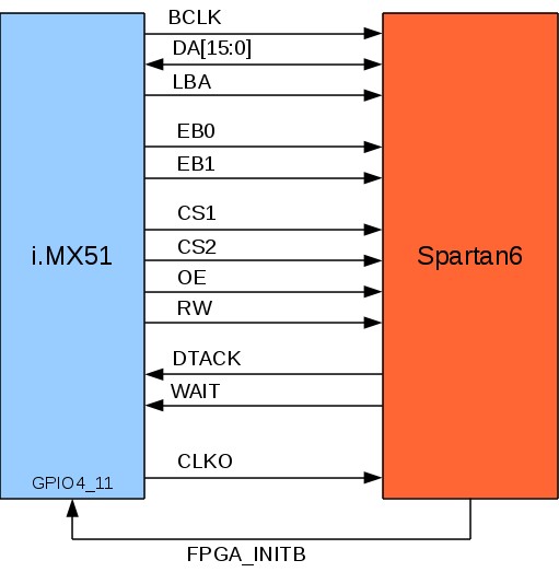
Figure 1 is a simplified view of APF51 schematics (page 15), signals are :
- BCLK: i.MX51 bulk clock used to clock the spartan6.
- DA[15:0] : Data/Address multiplexed bus.
- LBA : Noted ADV for ADdress Valid under the i.MX51 reference manual.
- EB0, EB1 : For Enable Byte, write signal for lower byte and upper byte on data bus.
- CS1 : Chip Select 1.
- CS2 : Chip Select 2.
- OE : For Output Enable bit, read signal. (Motorola way of bus)
- RW : Read/Write signal. (Intel way of bus)
- DTACK : Data acknoledge, for asynchronous access.
- WAIT : Wait signal used for some burst access.
Not part of WEIM bus :
- CLK0 : An i.MX51 output clock (not used ).
- FPGA_INITB : used by default for interrupts (GPIO4_11).
Signals in bold are signals used in default configuration.
Default configuration
By default the chip select 1 (CS1) is used for communication. The address domain corresponding to this chip select can be found in i.MX51 reference manual in chapter 2 (Memory Map page 65)
| Start Address | End Address | Size | Region |
|---|---|---|---|
| B800_0000 | BFFF_FFFF | 128M | CS1 (Flash) 128M |
| C000_0000 | C7FF_FFFF | 128M | CS2 (Flash) 128M |
