Difference between revisions of "APF27 FPGA-IMX interface description"
m (→Simulation) |
m (→Registers configuration) |
||
| Line 316: | Line 316: | ||
''Changing CLK0 to 100MHz:'' | ''Changing CLK0 to 100MHz:'' | ||
| + | To change CLK0 to 100MHz, we will use HCLK (400MHz) divided by 4. | ||
| + | |||
| + | Selecting HCLK (CCSR) | ||
| + | <pre class="apf"> | ||
| + | mw 10027028 00008305 # HCLK Source (MPLL 2x clock output / 3) := 400MHz | ||
| + | </pre> | ||
| + | |||
| + | Divide by 4 (PCDR0); | ||
| + | <pre class="apf"> | ||
| + | mw 10027018 12C41083 # divide by 4 | ||
| + | </pre> | ||
| + | |||
| + | And we have to add one more clock cycle for CS (CSCR5U): | ||
| + | <pre class="apf"> | ||
| + | mw.l D8002050 00000600 | ||
| + | </pre> | ||
===Timing register configuration=== | ===Timing register configuration=== | ||
Revision as of 16:46, 13 August 2009
This article describe the interface between IMX and Spartan3A on APF27. Documentation of i.MX interface can be found in the iMX reference manual, chapter 17, «Wireless External Interface Module (WEIM)».
Hardware
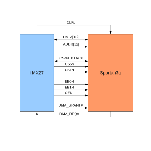
The detailled electronic schematics of apf27 fpga interface can be found on this document page 11. A simplified schema is shown below on figure 1.
The signals used in the design are:
- CLKO: Clock generated by i.MX. Used as general clock by the FPGA.
- DATA[16]: 16 bits data bus.
- ADDR[13]: 12 bits address bus, least significant bit (ADDR[0]) is not used because only word access are done.
- CS4N_DTACK: Chip Select 4 or Data Transmit ACKnowledge.
- CS5,CS1: Chip Select 5 and 1.
- EB0N and EB1N: For Enable Byte, write signal for lower byte and upper byte on data bus.
- OEN: For Output Enable bit, read signal.
- DMA_GRANT# and DMA_REQ#: Signals to use DMA on i.MX.
Each chip select has its own configuration (timing, address range, ...) that can be used for different slaves in the FPGA.
CLKO is by default configured to run at 133MHz to be synchronous with the WEIM bus that is internally clocked at 133MHz, too.
Chip Select Timings configuration
Present configuration (static timing)
The default configuration uses CS5 for accessing the FPGA. 32 bits register CS5 is used to configure all timing for this chip select. It's default configuration is:
- CS5U (Upper 16bits, see page 521 of reference manual ): mw D8002050 00000600
This will add 6 waits state on access to read value correctly (WSC: Wait State Control).
- CS5L (Lower 16bits,see page 525 of reference manual): mw D8002054 00000D01
Enable chip select (CSEN), Enable for only write access EB[] (EBC) and select data port size to 16bits (DSZ: Data port SiZe).
- CS5A (additionnal register, page 528): mw D8002058 0
- WCR (WEIM Configuration Register): mw D8002060 00002000
Address unshifted for CS5 (AUS5)
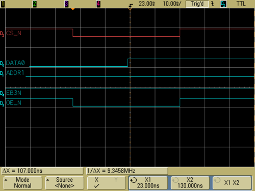
With this configuration, the access time (read/write) to the FPGA is set to 44ns.
This configuration is interesting because all timings are under control. But the problem is that to be perfectly synchronous, the FPGA is clocked at 133MHz like WEIM and some IP design doesn't work at this frequency.
Alternative configuration (with DTACK)
To solve the problem, another solution can be the DTACK signal (asynchronous protocol). The DTACK signal is emmited by the slave to master when write/read is done. With this solution, access time is variable and the timing is not static any more.
i.MX registers configuration
To configure CS5N access using dtack, the gpio PF21 must be configured on input with a_out :
md 10015500 1 # read direction register PTF_DDIR
md 10015510 1 # read register PTF_ICONFA2
By default, configuration is ok, we just have to select gpio in use :
mw 10015520 FFBF1E80 # PTF_GIUS
FPGA design
On design, the wishbone signal ack is returned to dtack pin. Here a sample code used to test the dtack :
library IEEE;
  use IEEE.std_logic_1164.all;
  use IEEE.numeric_std.all;

-- ----------------------------------------------------------------------------
    Entity imx27_wb16_wrapper is
-- ----------------------------------------------------------------------------
    port
    (
      -- i.MX Signals
      imx_address : in    std_logic_vector(11 downto 0);
      imx_data    : inout std_logic_vector(15 downto 0);
      imx_cs_n    : in    std_logic;
      imx_oe_n    : in    std_logic;
      imx_eb3_n   : in    std_logic;

      imx_dtack   : out   std_logic ;

      data0_out : out std_logic ;
      addr1_out : out std_logic ;
      cs_n_out  : out std_logic ;
      oe_n_out  : out std_logic ;
      eb3_n_out : out std_logic ;
      dtack_out : out std_logic ;

      -- Global Signals
      gls_reset : in std_logic;
      gls_clk   : in std_logic

    );
    end entity;

-- ----------------------------------------------------------------------------
    Architecture RTL of imx27_wb16_wrapper is
-- ----------------------------------------------------------------------------

    constant DELAY : natural := 2;

    signal write      : std_logic;
    signal read       : std_logic;
    signal strobe     : std_logic;
    signal writedata  : std_logic_vector(15 downto 0);
    signal address    : std_logic_vector(12 downto 0);

    signal reg1 : std_logic_vector(15 downto 0);
    signal reg2 : std_logic_vector(15 downto 0);

    signal write_ack : std_logic ;
    signal read_ack  : std_logic ;

    signal wbm_address  : std_logic_vector(12 downto 0);
    signal wbm_writedata: std_logic_vector(15 downto 0);
    signal wbm_readdata: std_logic_vector(15 downto 0);
    signal wbm_strobe   : std_logic ;
    signal wbm_write    : std_logic ;
    signal wbm_cycle    : std_logic ;

    signal dtack_s : std_logic ; -- dtack
    signal dtack_d : std_logic ; -- dtack delayed
    signal dtack_reg : std_logic_vector( DELAY-1 downto 0);
--i    signal dtack_old: std_logic_vector( DELAY-1 downto 0);
    signal dtack_old : std_logic ;

begin

    dtack_s <= write_ack or read_ack;

--    imx_dtack <= dtack_d;
--    dtack_out <= dtack_d;

    data0_out <= imx_data(0);
    addr1_out <= imx_address(1);
    cs_n_out  <= imx_cs_n;
    oe_n_out  <= imx_oe_n;
    eb3_n_out <= imx_eb3_n;

    -- ----------------------------------------------------------------------------
    --  External signals synchronization process
    -- ----------------------------------------------------------------------------
    process(gls_clk, gls_reset)
    begin
      if(gls_reset='1') then
        write   <= '0';
        read    <= '0';
        strobe  <= '0';
        writedata <= (others => '0');
        address   <= (others => '0');
      elsif(rising_edge(gls_clk)) then
        strobe  <= not (imx_cs_n) and not(imx_oe_n and imx_eb3_n);
        write   <= not (imx_cs_n or imx_eb3_n);
        read    <= not (imx_cs_n or imx_oe_n);
        address <= imx_address & '0';
        writedata <= imx_data;
      end if;
    end process;

    wbm_address    <= address when (strobe = '1') else (others => '0');
    wbm_writedata  <= writedata when (write = '1') else (others => '0');
    wbm_strobe     <= strobe;
    wbm_write      <= write;
    wbm_cycle      <= strobe;

    sync_p : process (gls_clk,gls_reset)
        variable ack: std_logic ;
    begin
        if gls_reset = '1' then
            imx_data <= (others => 'Z');
            imx_dtack <= '0';
            dtack_old <= '0';
        elsif rising_edge(gls_clk) then
            if read = '1' then
                imx_data <= wbm_readdata;
                dtack_old <= (read_ack or write_ack);
                imx_dtack <= dtack_old;
                dtack_out <= dtack_old;
            else
                imx_data <= (others => 'Z');
                dtack_old <= '0';
                imx_dtack <= '0';
                dtack_out <= '0';

            end if;

        end if;
    end process sync_p;


    register_write : process(gls_clk,gls_reset)
    begin
        if gls_reset = '1' then
            reg1 <= x"caca";
            reg2 <= x"5599";
        elsif rising_edge(gls_clk) then
            if (wbm_strobe = '1') and (wbm_cycle = '1') and (wbm_write = '1') then
                if wbm_address = "0000000000000" then
                    write_ack <= '1';
                    reg1 <= wbm_writedata;
                elsif wbm_address = "0000000000010" then
                    write_ack <= '1';
                    reg2 <= wbm_writedata;
                end if;
            else
                write_ack <= '0';
            end if;
        end if;
    end process register_write;

    register_read : process(gls_clk,gls_reset)
    begin
        if gls_reset = '1' then
            wbm_readdata <= (others => '0');
        elsif rising_edge(gls_clk) then
            if (wbm_strobe = '1') and (wbm_cycle = '1') and (wbm_write = '0') then
                if wbm_address = "0000000000000" then
                    read_ack <= '1';
                    wbm_readdata <= reg1;
                elsif wbm_address = "0000000000010" then
                    read_ack <= '1';
                    wbm_readdata <= reg2;
                end if;
            else
                read_ack <= '0';
            end if;
        end if;
    end process register_read;

end architecture RTL;
With ucf ;
# Constraint file
#
NET "gls_clk" TNM_NET = "gls_clk";
TIMESPEC "TS_rstgen_syscon00_ext_clk" = PERIOD "gls_clk" 7.5188 ns HIGH 50 %;

NET "gls_clk" LOC="N9" | IOSTANDARD=LVCMOS18;# CLK0
NET "imx_cs_n" LOC="P10" | IOSTANDARD=LVCMOS18;# CS5N
NET "imx_eb3_n" LOC="P9" | IOSTANDARD=LVCMOS18;# EB0N
NET "imx_oe_n" LOC="R9" | IOSTANDARD=LVCMOS18;# OEN
NET "imx_dtack" LOC="R3" | IOSTANDARD=LVCMOS18 | DRIVE=8;# CS4N_DTACK

NET "imx_address<0>" LOC="N5" | IOSTANDARD=LVCMOS18;# ADDR1
NET "imx_address<1>" LOC="L7" | IOSTANDARD=LVCMOS18;# ADDR2
NET "imx_address<2>" LOC="M7" | IOSTANDARD=LVCMOS18;# ADDR3
NET "imx_address<3>" LOC="M8" | IOSTANDARD=LVCMOS18;# ADDR4
NET "imx_address<4>" LOC="L8" | IOSTANDARD=LVCMOS18;# ADDR5
NET "imx_address<5>" LOC="L9" | IOSTANDARD=LVCMOS18;# ADDR6
NET "imx_address<6>" LOC="L10" | IOSTANDARD=LVCMOS18;# ADDR7
NET "imx_address<7>" LOC="M11" | IOSTANDARD=LVCMOS18;# ADDR8
NET "imx_address<8>" LOC="P11" | IOSTANDARD=LVCMOS18;# ADDR9
NET "imx_address<9>" LOC="N11" | IOSTANDARD=LVCMOS18;# ADDR10
NET "imx_address<10>" LOC="N12" | IOSTANDARD=LVCMOS18;# ADDR11
NET "imx_address<11>" LOC="P13" | IOSTANDARD=LVCMOS18;# ADDR12

NET "imx_data<0>" LOC="T5" | IOSTANDARD=LVCMOS18 | DRIVE=8;# DATA0
NET "imx_data<1>" LOC="T6" | IOSTANDARD=LVCMOS18 | DRIVE=8;# DATA1
NET "imx_data<2>" LOC="P7" | IOSTANDARD=LVCMOS18 | DRIVE=8;# DATA2
NET "imx_data<3>" LOC="N8" | IOSTANDARD=LVCMOS18 | DRIVE=8;# DATA3
NET "imx_data<4>" LOC="P12" | IOSTANDARD=LVCMOS18 | DRIVE=8;# DATA4
NET "imx_data<5>" LOC="T13" | IOSTANDARD=LVCMOS18 | DRIVE=8;# DATA5
NET "imx_data<6>" LOC="R13" | IOSTANDARD=LVCMOS18 | DRIVE=8;# DATA6
NET "imx_data<7>" LOC="T14" | IOSTANDARD=LVCMOS18 | DRIVE=8;# DATA7
NET "imx_data<8>" LOC="P5" | IOSTANDARD=LVCMOS18 | DRIVE=8;# DATA8
NET "imx_data<9>" LOC="N6" | IOSTANDARD=LVCMOS18 | DRIVE=8;# DATA9
NET "imx_data<10>" LOC="T3" | IOSTANDARD=LVCMOS18 | DRIVE=8;# DATA10
NET "imx_data<11>" LOC="T11" | IOSTANDARD=LVCMOS18 | DRIVE=8;# DATA11
NET "imx_data<12>" LOC="T4" | IOSTANDARD=LVCMOS18 | DRIVE=8;# DATA12
NET "imx_data<13>" LOC="R5" | IOSTANDARD=LVCMOS18 | DRIVE=8;# DATA13
NET "imx_data<14>" LOC="M10" | IOSTANDARD=LVCMOS18 | DRIVE=8;# DATA14
NET "imx_data<15>" LOC="T10" | IOSTANDARD=LVCMOS18 | DRIVE=8;# DATA15

NET "data0_out" LOC="D16" | IOSTANDARD=LVCMOS18 | DRIVE=12;#IO_L22P_1
NET "addr1_out" LOC="D15" | IOSTANDARD=LVCMOS18 | DRIVE=12;#IO_L22N_1
NET "cs_n_out"  LOC="N3"  | IOSTANDARD=LVCMOS18 | DRIVE=12;#IO_L24P_3
NET "oe_n_out"  LOC="R1"  | IOSTANDARD=LVCMOS18 | DRIVE=12;#IO_L23P_3
NET "eb3_n_out" LOC="N2"  | IOSTANDARD=LVCMOS18 | DRIVE=12;#IO_L22P_3
NET "dtack_out" LOC="M1"  | IOSTANDARD=LVCMOS18 | DRIVE=8;#IO_L20P_3

#end
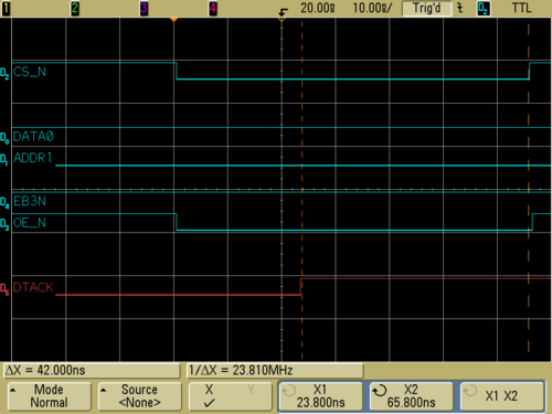
Timings
The main problem with this solution is that i.MX wait a too long time (~42ns) after dtack rise to de-assert its chip select.
Synchronous access with FPGA at 100MHz
The main problem with fpga clocked at 100MHz is that wishbone will not be synchronous with WEIM interface (clocked at 133MHz).
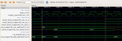
Simulation
To unsure that interface work well, we will simulate it. To reproduce this simulation, ask User:FabienM that will give you the project (~/podtree/trunk/src/tests/testbus).
Registers configuration
Changing CLK0 to 100MHz: To change CLK0 to 100MHz, we will use HCLK (400MHz) divided by 4.
Selecting HCLK (CCSR)
mw 10027028 00008305 # HCLK Source (MPLL 2x clock output / 3) := 400MHz
Divide by 4 (PCDR0);
mw 10027018 12C41083 # divide by 4
And we have to add one more clock cycle for CS (CSCR5U):
mw.l D8002050 00000600
Timing register configuration
All register configurations for external memory are done in u-boot. Configuration file can be found in buildroot/project_build_armv5te/<project_name>/u-boot-1.3.4/include/configs/apf27.h And is saved in armadeus tree at buildroot/target/device/armadeus/apf27/apf27.h


