Difference between revisions of "IMX51-Spartan6 interface description"
From ArmadeusWiki
| Line 4: | Line 4: | ||
Figure 1 is a simplified view of [[Datasheet#APF51 | APF51 schematics]] (page 15), signals are : | Figure 1 is a simplified view of [[Datasheet#APF51 | APF51 schematics]] (page 15), signals are : | ||
| + | |||
| + | * BCLK: i.MX51 bulk clock used to clock the spartan6. | ||
| + | * DA[15:0] : Data/Address multiplexed bus. | ||
| + | * LBA : Noted ADV for '''AD'''dress '''V'''alid under the i.MX51 reference manual. | ||
| + | * EB0, EB1 : For Enable Byte, write signal for lower byte and upper byte on data bus. | ||
| + | * CS1 : Chip Select 1. | ||
| + | * CS2 : Chip Select 2. | ||
| + | * OE : For Output Enable bit, read signal. (Motorola way of bus) | ||
| + | * RW : Read/Write signal. (Intel way of bus) | ||
| + | * DTACK : Data acknoledge, for asynchronous access. | ||
| + | * WAIT : Wait signal used for some burst access. | ||
| + | Not part of WEIM bus : | ||
| + | * CLK0 : An i.MX51 output clock (not used ). | ||
| + | * FPGA_INITB : used by default for interrupts (GPIO4_11). | ||
Revision as of 12:46, 13 January 2012
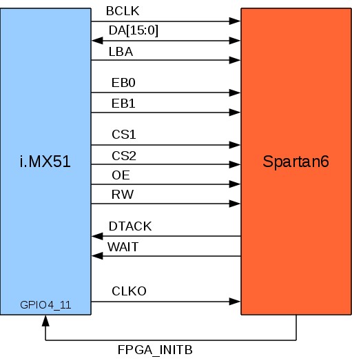
This article describe the bus interface configuration to communicate between i.MX51 processor and Spartan6 FPGA.
Figure 1 is a simplified view of APF51 schematics (page 15), signals are :
- BCLK: i.MX51 bulk clock used to clock the spartan6.
- DA[15:0] : Data/Address multiplexed bus.
- LBA : Noted ADV for ADdress Valid under the i.MX51 reference manual.
- EB0, EB1 : For Enable Byte, write signal for lower byte and upper byte on data bus.
- CS1 : Chip Select 1.
- CS2 : Chip Select 2.
- OE : For Output Enable bit, read signal. (Motorola way of bus)
- RW : Read/Write signal. (Intel way of bus)
- DTACK : Data acknoledge, for asynchronous access.
- WAIT : Wait signal used for some burst access.
Not part of WEIM bus :
- CLK0 : An i.MX51 output clock (not used ).
- FPGA_INITB : used by default for interrupts (GPIO4_11).
